| |
|

|
|
|
|
| |
|
|
| |
 |
Diode Logic
|
|
|
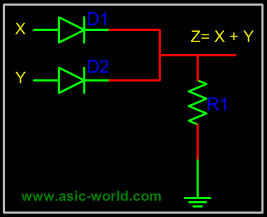
In DL (diode logic), all the logic is implemented using diodes and resistors. One basic thing about the diode, is that diode needs to be forward biased to conduct. Below is the example of a few DL logic circuits. |
| |
|
|
|
|
 |
| |
|
|
|
|
When no input is connected or driven, output Z is low, due to resistor R1. When high is applied to either X or Y, or both X and Y are driven high, the corresponding diode get forward biased and thus conducts. When any diode conducts, output Z goes high. |
| |
|
|
|
|
Points to Ponder |
|
|
- Diode Logic suffers from voltage degradation from one stage to the next.
- Diode Logic only permits OR and AND functions.
- Diode Logic is used extensively but not in integrated circuits.
|
| |
|
|
| |
|
Resistor Transistor Logic
|
|
|
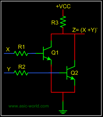
In RTL (resistor transistor logic), all the logic are implemented using resistors and transistors. One basic thing about the transistor (NPN), is that HIGH at input causes output to be LOW (i.e. like a inverter). Below is the example of a few RTL logic circuits. |
| |
|
|
|
|
 |
| |
|
|
|
|
A basic circuit of an RTL NOR gate consists of two transistors Q1 and Q2, connected as shown in the figure above. When either input X or Y is driven HIGH, the corresponding transistor goes to saturation and output Z is pulled to LOW. |
| |
|
|
|
|
|
| |
|
|
| |
|
Diode Transistor Logic
|
| |
|
|
|
|
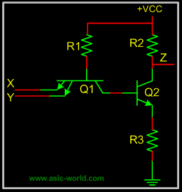
In DTL (Diode transistor logic), all the logic is implemented using diodes and transistors. A basic circuit in the DTL logic family is as shown in the figure below. Each input is associated with one diode. The diodes and the 4.7K resistor form an AND gate. If input X, Y or Z is low, the corresponding diode conducts current, through the 4.7K resistor. Thus there is no current through the diodes connected in series to transistor base . Hence the transistor does not conduct, thus remains in cut-off, and output out is High. |
| |
|
|
|
|
If all the inputs X, Y, Z are driven high, the diodes in series conduct, driving the transistor into saturation. Thus output out is Low. |
| |
|
|
|
|
 |
| |
|
|
| |
|
Transistor Transistor Logic
|
|
|
In Transistor Transistor logic or just TTL, logic gates are built only around transistors. TTL was developed in 1965. Through the years basic TTL has been improved to meet performance requirements. There are many versions or families of TTL. |
| |
|
|
|
|
- Standard TTL.
- High Speed TTL
- Low Power TTL.
- Schhottky TTL.
|
| |
|
|
|
|
Here we will discuss only basic TTL as of now; maybe in the future I will add more details about other TTL versions. As such all TTL families have three configurations for outputs. |
| |
|
|
|
|
- Totem - Pole output.
- Open Collector Output.
- Tristate Output.
|
| |
|
|
|
|
Before we discuss the output stage let's look at the input stage, which is used with almost all versions of TTL. This consists of an input transistor and a phase splitter transistor. Input stage consists of a multi emitter transistor as shown in the figure below. When any input is driven low, the emitter base junction is forward biased and input transistor conducts. This in turn drives the phase splitter transistor into cut-off. |
| |
|
|
|
|
 |
| |
|
|
| |
 |
Totem - Pole Output
|
|
|
Below is the circuit of a totem-pole NAND gate, which has got three stages. |
| |
|
|
|
|
- Input Stage
- Phase Splitter Stage
- Output Stage
|
| |
|
|
|
|
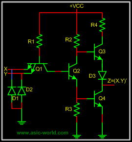
Input stage and Phase splitter stage have already been discussed. Output stage is called Totem-Pole because transistor Q3 sits upon Q4. |
| |
|
|
|
|
Q2 provides complementary voltages for the output transistors Q3 and Q4, which stack one above the other in such a way that while one of these conducts, the other is in cut-off. |
| |
|
|
|
|
Q4 is called pull-down transistor, as it pulls the output voltage down, when it saturates and the other is in cut-off (i.e. Q3 is in cut-off). Q3 is called pull-up transistor, as it pulls the output voltage up, when it saturates and the other is in cut-off (i.e. Q4 is in cut-off). |
| |
|
|
|
|
Diodes in input are protection diodes which conduct when there is large negative voltage at input, shorting it to the ground. |
| |
|
|
|
|
 |
| |
|
|
| |
|
Tristate Output.
|
|
|
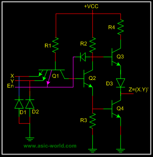
Normally when we have to implement shared bus systems inside an ASIC or externally to the chip, we have two options: either to use a MUX/DEMUX based system or to use a tri-state base bus system. |
| |
|
|
|
|
In the latter, when logic is not driving its output, it does not drive LOW neither HIGH, which means that logic output is floating. Well, one may ask, why not just use an open collector for shared bus systems? The problem is that open collectors are not so good for implementing wire-ANDs. |
| |
|
|
|
|
The circuit below is a tri-state NAND gate; when Enable En is HIGH, it works like any other NAND gate. But when Enable En is driven LOW, Q1 Conducts, and the diode connecting Q1 emitter and Q2 collector, conducts driving Q3 into cut-off. Since Q2 is not conducting, Q4 is also at cut-off. When both pull-up and pull-down transistors are not conducting, output Z is in high-impedance state. |
| |
|
|
|
|
 |
| |
|
|
|
|
Note : I will try to add more details when I find time. |
| |
|
|
| |
|
|
| |
|
|
|
|
|
| |
|
|