| |
|

|
|
|
|
| |
|
|
| |
 |
Digital Logic Families.
|
|
|
Logic families can be classified broadly according to the technologies they are built using. In earlier days we had vast number of this technologies, like in list below. |
| |
|
|
|
|
- DL : Diode Logic.
- RTL : Resistor Transistor Logic.
- DTL : Diode Transistor Logic.
- HTL : High threshold Logic.
- TTL : Transistor Transistor Logic.
- I2L : Integrated Injection Logic.
- ECL: Emitter coupled logic.
- MOS: Metal Oxide Semiconductor Logic ( PMOS and NMOS).
- CMOS : Complimentary Metal Oxide Semiconductor Logic.
|
| |
|
|
|
|
Of this, only CMOS is most widely used by the ASIC (Chip) designers, we will still try to understand few of the extinct technologies and lesser used technologies. More in depth explanation of CMOS will be covered in VLSI section. |
| |
|
|
| |
 |
Basic Concepts
|
| |
|
|
|
|
Before we start looking at the how gates are built using various technologies, we need to understand few basic concepts. This concepts will go long way i.e if you become a ASIC designer or Board designer, you may need to know this concepts very well. |
| |
|
|
|
|
- Fan-in.
- Fan-out.
- Noise Margin.
- Power Dissipation.
- Gate Delay.
- Wire Delay.
- Skew.
- Voltage Threshold.
|
| |
|
|
| |
 |
Fan-in
|
|
|
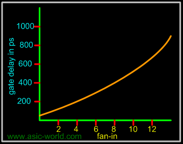
Fan-in is number of inputs a gate has, Like a two input AND gate has fan-in of two, a three input NAND gate as a fan-in of three. So a NOT gate always has a fan-in of one. Below figure shows the effect of Fan-in on the delay offered by gate for a CMOS based gate. Normally delay increases quadratic function of fan-in. |
| |
|
|
|
|
 |
| |
|
|
| |
|
Fan-out
|
|
|
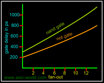
The number of gates that each gate can drive, while providing voltage levels in the guaranteed range is called the standard load or fan-out. The fan-out really depends on the amount of electric current a gate can source or sink while driving other gates. The effects of loading a logic gate output with more than its rated fan-out has the following effects. |
| |
|
|
|
|
- In the LOW state the output voltage VOL may increase above VOLmax.
- In the HIGH state the output voltage VOH may decrease below VOHmin.
- The operating temperature of the device may increase thereby reducing the reliability of the device and eventually causing the device failure.
- Output rise and fall times may increase beyond specifications
- The propagation delay may rise above the specified value.
|
| |
|
|
|
|
Normally as in the case of fan-in, delay offered by a gate increases with increase in fan-out. |
| |
|
|
|
|
 |
| |
|
|
| |
|
Gate Delay
|
|
|
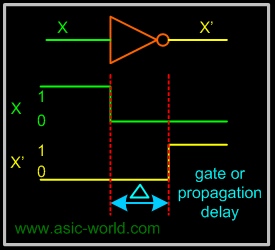
Gate delay is delay offered by gate for signal appearing at its input, before it reached gates output. Below figure shows a NOT gate with a gate delay of "Delta", Where output X' changes only after a delay of "delta". Gate delay is also know as propagation delay. |
| |
|
|
|
|
 |
| |
|
|
|
|
Gate delay is not same for both the transition, i.e gate delay will be different for low to high transition, compared to high to low transition. |
| |
|
|
|
|
Low to high transition is called turn-on delay and High to low transition is called turn-off delay. |
| |
|
|
| |
|
Wire Delay
|
|
|
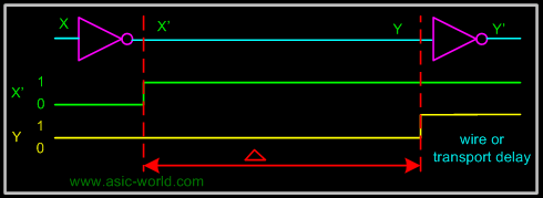
Gates are connected together with wires and this wires do delay the signal they carry, this delays become very signification with increase in frequency, say when the when transistor size's are sub-micron. Sometimes wire delay is also called as flight time (i.e. signal flight time from point A to B). Wire delay is also knows as transport delay. |
| |
|
|
|
|
 |
| |
|
|
|
|
|
| |
|
|
| |
|
Skew
|
|
|
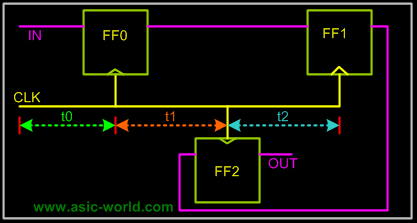
Same signal arriving at different parts of design with different phase is know as skew. Skew normally referred to clock signals. In the below figure, clock signal CLK reached flip-flop FF0 at time t0, so with respect to clock phase at the source to the clock at FF0 input has a clock slew of t0 time units. Normally this is in nano seconds. |
| |
|
|
|
|
 |
| |
|
|
|
|
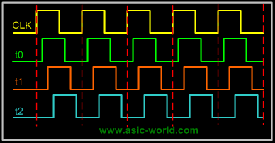
Below waveform shows, how clock looks at different parts of the design. We will discuss the effects of clock skew later. |
| |
|
|
|
|
 |
| |
|
|
| |
|
Logic levels
|
|
|
Logic levels are the voltage levels for logic high and logic low. |
| |
|
|
|
|
- VOHmin : The minimum output voltage in HIGH state (logic '1'). VOHmin is 2.4 V for TTL and 4.9 V for CMOS.
- VOLmax : The maximum output voltage in LOW state (logic '0'). VOLmax is 0.4 V for TTL and 0.1 V for CMOS.
- VIHmin : The minimum input voltage guaranteed to be recognised as logic 1. VIHmin is 2 V for TTL and 3.5 V for CMOS.
- VILmax : The maximum input voltage guaranteed to be recognised as logic 0. VILmax is 0.8 V for TTL and 1.5 V for CMOS.
|
| |
|
|
| |
|
Current levels
|
| |
|
|
|
|
- IOHmin: The maximum current the output can source in HIGH state while still maintaining the output voltage above VOHmin.
- IOLmax : The maximum current the output can sink in LOW state while still maintaining the output voltage below VOLmax.
- IImax : The maximum current that flows into an input in any state (1µA for CMOS).
|
| |
|
|
| |
|
Noise Margin
|
|
|
Gate circuits are constructed to sustain variations in input and output voltage levels. Variations are usually result of several different factors. |
| |
|
|
|
|
- Batteries lose their full potential, causing the supply voltage to drop
- High operating temperatures may cause a drift in transistor voltage and current characteristics
- Spurious pulses may be introduced on signal lines by normal surges of current in neighboring supply lines.
|
| |
|
|
|
|
All these undesirable voltage variations that are superimposed on normal operating voltage levels are called noise. All gates designed to tolerate a certain amount of noise on their input and output ports. The maximum noise voltage level that is tolerated by a gate is called a noise margin. Noise margin derived from I/P-O/P voltage characteristic, Measured under different operating conditions. Normally supplied in documentation about gate from manufacturer. |
| |
|
|
|
|
- LNM (Low noise margin): The largest noise amplitude that is guaranteed not change the output voltage level when superimposed on the input voltage of the logic gate (when this voltage is in the LOW interval). LNM=VILmax-VOlmax.
- HNM (High noise margin): The largest noise amplitude that is guaranteed not change the output voltage level if superimposed on the input voltage of the logic gate (when this voltage is in the HIGH interval). HNM=VOHmin-VIHmin
|
| |
|
|
| |
|
tr (Rise time)
|
|
|
The time required for the output voltage to increase from VILmax to VIHmin. |
| |
|
|
| |
|
tf (Fall time)
|
|
|
The time required for the output voltage to decrease from VIHmin to VILmax. |
| |
|
|
| |
|
tp (Propagation delay)
|
|
|
The time between the logic transition on an input and the corresponding logic transition on the output of the logic gate. The propagation delay is measured at midpoints. |
| |
|
|
| |
|
Power Dissipation.
|
|
|
Each gate is connected to a power supply VCC (VDD in the case of CMOS). Draws a certain amount of current during its operation. Since each gate can be in a High state, Transition or Low state, There are three distinguish currents drawn from power supply. |
| |
|
|
|
|
- ICCH : Current drawn during HIGH state.
- ICCT: Current drawn during HIGH to LOW, LOW to HIGH Transition.
- ICCL : Current drawn during LOW state.
|
| |
|
|
|
|
For TTL, ICCT the transition current is negligible, in comparison to ICCH and ICCL. If we assume that ICCH and ICCL are equal then, |
| |
|
|
|
|
Average Power Dissipation = Vcc * (ICCH + ICCL)/2 |
| |
|
|
|
|
For CMOS, ICCH and ICCL current is negligible, in comparison to ICCT. So the Average power dissipation is calculated as below. |
| |
|
|
|
|
Average Power Dissipation = Vcc * ICCT. |
| |
|
|
|
|
So for TTL like logics family, power dissipation does not depend on frequency of operation, and for CMOS the power dissipation depends on the operation frequency. |
| |
|
|
|
|
Power Dissipation is an important metric for two reasons. Amount of current and power available in a battery is nearly constant. Power dissipation of a circuit or system defines battery life, The greater the power dissipation, the shorter the battery life. Power dissipation is proportional to the heat generated by the chip or system, Excessive heat dissipation may increase operating temperature and cause gate circuitry to drift out of its normal operating range, will cause gates to generate improper output values. Thus power dissipation of any gate implementation must be kept as low as possible. |
| |
|
|
|
|
Other this, power dissipation can be classified into static power dissipation and Dynamic power dissipation. |
| |
|
|
|
|
- Ps (Static Power Dissipation) : Power consumed when the output or input are not changing or rather when clock is turned off. Normally static power dissipation is caused by leakage current. (As we reduce the transistor size, i.e. below 90nm, leakage current could be as high as 40% of total power dissipation).
- Pd (Dynamic Power Dissipation) : Power consumed during output and input transitions, So we can say Pd is actual power i.e. power consumed by transistors + leakage current.
|
| |
|
|
|
|
Thus total power dissipation is |
| |
|
|
|
|
Total power dissipation = static power dissipation + dynamic power dissipation. |
| |
|
|
| |
|
|
|
|
|
| |
|
|
| |
|
|